
 Technology peripherals
It Industry
Samsung starts mass production of its first batch of ninth-generation V-NAND flash memory
Technology peripherals
It Industry
Samsung starts mass production of its first batch of ninth-generation V-NAND flash memory
Samsung starts mass production of its first batch of ninth-generation V-NAND flash memory

News from this site on April 23, Samsung Semiconductor announced today that its ninth-generation V-NAND 1Tb TLC product has begun mass production, which has a bit density that is approximately 50% higher than Samsung’s previous generation product, improve production efficiency through channel hole etching technology.

With Samsung’s smallest cell size and thinnest stack thickness, Samsung’s ninth-generation V-NAND’s bit density ratio The eighth generation V-NAND has improved by about 50%. The application of new technical features such as cell interference avoidance and cell life extension improves product quality and reliability, while the elimination of virtual channel holes significantly reduces the memory cell planar area.
In addition, Samsung’s “channel hole etching” technology creates electronic pathways by stacking mold layers, drilling holes simultaneously in a dual-layer structure to achieve Samsung’s highest number of unit layers, thereby maximizing Manufacturing productivity. As the number of cell layers increases, the ability to penetrate more cells becomes critical, which places requirements on more complex etching techniques.
The ninth-generation V-NAND is equipped with the next-generation NAND flash memory interface "Toggle 5.1", which can increase data input/output speed by 33%, up to 3.2 gigabits per second (Gbps). In addition to this new interface, Samsung also plans to solidify its position in the high-performance SSD market by expanding support for PCIe 5.0.
Based on Samsung’s progress in low-power design, the ninth-generation V-NAND also reduces power consumption by 10% compared to the previous generation.
Samsung has started mass production of its ninth-generation V-NAND 1Tb TLC products this month, and will start mass production of its fourth-generation quad-layer cell (QLC) ninth-generation V-NAND## in the second half of this year. #.
Korean media Hankyung said that the number of stacking layers of Samsung’s 9th generation V-NAND flash memory is 290. However, earlier reports on this site mentioned that Samsung demonstrated a 280-layer stacked QLC flash memory at an academic conference. Semiconductor industry observer TechInsights said Samsung’s 10th generation V-NAND flash memory is expected to reach 430 layers, further improving stacking advantages.The above is the detailed content of Samsung starts mass production of its first batch of ninth-generation V-NAND flash memory. For more information, please follow other related articles on the PHP Chinese website!

Hot AI Tools

Undresser.AI Undress
AI-powered app for creating realistic nude photos

AI Clothes Remover
Online AI tool for removing clothes from photos.

Undress AI Tool
Undress images for free

Clothoff.io
AI clothes remover

Video Face Swap
Swap faces in any video effortlessly with our completely free AI face swap tool!

Hot Article
Hot Tools

Notepad++7.3.1
Easy-to-use and free code editor

SublimeText3 Chinese version
Chinese version, very easy to use

Zend Studio 13.0.1
Powerful PHP integrated development environment

Dreamweaver CS6
Visual web development tools

SublimeText3 Mac version
God-level code editing software (SublimeText3)
Hot Topics


 Industry's highest transfer rate of 3.6GB/s, Micron announces mass production of ninth-generation 276-layer TLC NAND flash memory
Jul 31, 2024 am 08:05 AM
Industry's highest transfer rate of 3.6GB/s, Micron announces mass production of ninth-generation 276-layer TLC NAND flash memory
Jul 31, 2024 am 08:05 AM
According to news from this site on July 30, Micron announced today (local time) that its ninth generation (site note: 276 layers) 3DTLC NAND flash memory will be mass-produced and shipped. Micron said that its G9NAND has the industry's highest I/O transfer rate of 3.6GB/s (i.e. 3600MT/s flash memory interface rate), which is 50% higher than the existing competing products of 2400MT/s, and can better meet the needs of data-intensive workloads. High throughput requirements. At the same time, Micron's G9NAND is 99% and 88% higher than other solutions on the market in terms of write bandwidth and read bandwidth respectively. This NAND particle-level advantage will bring performance and energy efficiency to solid-state drives and embedded storage solutions. improvement. In addition, like previous generations of Micron NAND flash memory, Micron 276
 Samsung's 9th generation V-NAND metal wiring mass production process is revealed to use molybdenum technology for the first time
Jul 03, 2024 pm 05:39 PM
Samsung's 9th generation V-NAND metal wiring mass production process is revealed to use molybdenum technology for the first time
Jul 03, 2024 pm 05:39 PM
According to news from this site on July 3, according to Korean media TheElec, Samsung tried to use molybdenum (Mo) for the first time in the "metal wiring" (metalwiring) of its 9th generation V-NAND. Note from this site: The eight major processes in the semiconductor manufacturing process are: wafer manufacturing oxidation photolithography etching deposition metal wiring testing packaging metal wiring process mainly uses different methods to connect billions of electronic components to form different semiconductors (CPU , GPU, etc.), it can be said to "inject life into semiconductors." Sources say Samsung has introduced five Mo deposition machines from Lam Research, and plans to introduce 20 more pieces of equipment next year. In addition to Samsung Electronics, companies such as SK Hynix, Micron and Kioxia are also
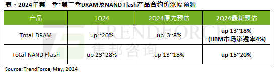 The impact of the AI wave is obvious. TrendForce has revised up its forecast for DRAM memory and NAND flash memory contract price increases this quarter.
May 07, 2024 pm 09:58 PM
The impact of the AI wave is obvious. TrendForce has revised up its forecast for DRAM memory and NAND flash memory contract price increases this quarter.
May 07, 2024 pm 09:58 PM
According to a TrendForce survey report, the AI wave has a significant impact on the DRAM memory and NAND flash memory markets. In this site’s news on May 7, TrendForce said in its latest research report today that the agency has increased the contract price increases for two types of storage products this quarter. Specifically, TrendForce originally estimated that the DRAM memory contract price in the second quarter of 2024 will increase by 3~8%, and now estimates it at 13~18%; in terms of NAND flash memory, the original estimate will increase by 13~18%, and the new estimate is 15%. ~20%, only eMMC/UFS has a lower increase of 10%. ▲Image source TrendForce TrendForce stated that the agency originally expected to continue to
 SK Hynix takes the lead in demonstrating UFS 4.1 universal flash memory, based on V9 TLC NAND particles
Aug 09, 2024 am 10:42 AM
SK Hynix takes the lead in demonstrating UFS 4.1 universal flash memory, based on V9 TLC NAND particles
Aug 09, 2024 am 10:42 AM
According to news from this website on August 9, according to a press release issued by SK Hynix yesterday local time, the company demonstrated a series of new storage products at the FMS2024 Summit, including USF4.1 universal flash memory that has not yet officially released specifications. According to the official website of the JEDEC Solid State Technology Association, the latest UFS specification currently announced is UFS4.0 in August 2022. UFS4.0 specifies a theoretical interface speed of up to 46.4Gbps for each device, and USF4.1 is expected to further improve the transmission rate. ▲JEDECUFS specification page SK Hynix demonstrated two UFS4.1 general-purpose flash memories with capacities of 512GB and 1TB respectively, both based on the 321-layer stacked V91TbTLCNAND flash memory.
 It is reported that Samsung Electronics V9 QLC NAND flash memory has not yet received mass production-ready license, affecting Pyeongtaek P4 factory planning
Jul 31, 2024 pm 08:38 PM
It is reported that Samsung Electronics V9 QLC NAND flash memory has not yet received mass production-ready license, affecting Pyeongtaek P4 factory planning
Jul 31, 2024 pm 08:38 PM
According to news from this site on July 31, Korean media ZDNetKorea reported that the QLC version of Samsung Electronics’ V9NAND flash memory has not yet received a mass production license, which has affected the production line construction planning of the Pyeongtaek P4 factory. Samsung Electronics announced in April this year that the 1Tb capacity TLC version of its V9NAND flash memory has achieved mass production, and the corresponding QLC version will enter mass production in the second half of this year. However, until now, Samsung Electronics has not issued a PRA (this site's note: should refer to Production Readiness Approval) mass production-ready license for V9QLCNAND flash memory. QLC flash memory with higher capacity and lower cost is currently the hot spot for AI inference server storage needs. The future of star products is unclear, making the three
 Apple iPhone will use QLC flash memory with lower lifespan/performance
Jul 26, 2024 am 01:52 AM
Apple iPhone will use QLC flash memory with lower lifespan/performance
Jul 26, 2024 am 01:52 AM
According to foreign media reports, Apple will enable a larger storage design on the new iPhone released in 2026, which is expected to be 2TB. In addition, it is reported that Apple will use QLCNAND flash memory, possibly to control costs. 1. Changes in storage capacity According to news, Apple may change the storage capacity on iPhone 16. Instead of triple-level cell (TLC) NAND flash, quad-level cell (QLC) NAND flash will be used on models with storage capacities of 1TB or more. 2. Advantages of QLC flash memory Compared with TLC, the advantage of QLC is that each storage unit can store four bits of data. Store more data than TLC when using the same number of cells, or use fewer cells to store more data
 Sources say Samsung Electronics will mass-produce 9th generation V-NAND flash memory as soon as later this month
Apr 12, 2024 pm 01:50 PM
Sources say Samsung Electronics will mass-produce 9th generation V-NAND flash memory as soon as later this month
Apr 12, 2024 pm 01:50 PM
According to news from this site on April 12, Korean media Hankyung reported that Samsung will achieve mass production of 9th generation V-NAND flash memory as soon as later this month. Samsung executive Jung-Bae Lee said in October last year that its next-generation NAND flash memory will be mass-produced "early this year" and will have an industry-leading number of stacking layers. Samsung mass-produced 236-layer 8th-generation V-NAND in November 2022, which means that the interval between the two generations is about a year and a half. ▲Samsung’s 8th generation V-NAND flash memory Hankyung said that the number of stacking layers of the 9th generation V-NAND flash memory will be 290. However, earlier reports on this site mentioned that Samsung demonstrated a 280-layer stacked QLC flash memory at an academic conference. , the flash IO interface rate reaches 3.2G
 Samsung starts mass production of its first batch of ninth-generation V-NAND flash memory
Apr 23, 2024 pm 05:37 PM
Samsung starts mass production of its first batch of ninth-generation V-NAND flash memory
Apr 23, 2024 pm 05:37 PM
According to news from this website on April 23, Samsung Semiconductor announced today that its ninth-generation V-NAND1TbTLC product has begun mass production, which has a bit density that is approximately 50% higher than Samsung’s previous generation product and is improved through channel hole etching technology. Productivity. With Samsung’s smallest cell size and thinnest stack thickness currently, Samsung’s ninth-generation V-NAND’s bit density is about 50% higher than its eighth-generation V-NAND. The application of new technical features such as cell interference avoidance and cell life extension improves product quality and reliability, while the elimination of virtual channel holes significantly reduces the memory cell planar area. In addition, Samsung’s “via hole etching” technology creates circuits by stacking mold layers.
