
 Technology peripherals
It Industry
Samsung Electronics reiterates that the SF1.4 process is expected to be mass-produced in 2027 and plans to enter the field of co-packaging optics
Technology peripherals
It Industry
Samsung Electronics reiterates that the SF1.4 process is expected to be mass-produced in 2027 and plans to enter the field of co-packaging optics
Samsung Electronics reiterates that the SF1.4 process is expected to be mass-produced in 2027 and plans to enter the field of co-packaging optics

According to news from this site on June 13, Samsung Electronics reiterated at the Samsung Foundry Forum 2024 North America held on June 12, local time, that its SF1.4 process is expected to be mass-produced in 2027, countering previous media rumors. .
Samsung said its 1.4nm-level process preparations are progressing smoothly, and is expected to reach mass production milestones in terms of performance and yield in 2027.
In addition, Samsung Electronics is actively researching advanced logic process technology in the post-1.4nm era through innovations in materials and structures to realize Samsung's commitment to continuously surpass Moore's Law.
Samsung Electronics simultaneously confirmed that it still plans to mass produce the second-generation 3nm process SF3 in the second half of 2024.
In the more traditional FinFET transistor part, Samsung Electronics plans to launch the SF4U process in 2025. This node will further enhance competitiveness in terms of PPA metrics through optical shrinkage.

Cui Shirong, head of the Foundry Business Department of Samsung Electronics, also said:
We still plan to launch products for high-speed, low-speed Integrated co-packaged optics (CPO) technology for power data processing provides customers with the one-stop artificial intelligence solutions they need to thrive in this transformative era.
This site has reported earlier that in addition to Intel, which has accumulated deep experience in the field of optoelectronics, TSMC, another member of the three advanced process giants, also plans to launch a joint venture based on COUPE technology integration in 2026. Packaged optical module.
The above is the detailed content of Samsung Electronics reiterates that the SF1.4 process is expected to be mass-produced in 2027 and plans to enter the field of co-packaging optics. For more information, please follow other related articles on the PHP Chinese website!

Hot AI Tools

Undresser.AI Undress
AI-powered app for creating realistic nude photos

AI Clothes Remover
Online AI tool for removing clothes from photos.

Undress AI Tool
Undress images for free

Clothoff.io
AI clothes remover

Video Face Swap
Swap faces in any video effortlessly with our completely free AI face swap tool!

Hot Article
Hot Tools

Notepad++7.3.1
Easy-to-use and free code editor

SublimeText3 Chinese version
Chinese version, very easy to use

Zend Studio 13.0.1
Powerful PHP integrated development environment

Dreamweaver CS6
Visual web development tools

SublimeText3 Mac version
God-level code editing software (SublimeText3)
Hot Topics


 Sources say Samsung Electronics and SK Hynix will commercialize stacked mobile memory after 2026
Sep 03, 2024 pm 02:15 PM
Sources say Samsung Electronics and SK Hynix will commercialize stacked mobile memory after 2026
Sep 03, 2024 pm 02:15 PM
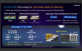
According to news from this website on September 3, Korean media etnews reported yesterday (local time) that Samsung Electronics and SK Hynix’s “HBM-like” stacked structure mobile memory products will be commercialized after 2026. Sources said that the two Korean memory giants regard stacked mobile memory as an important source of future revenue and plan to expand "HBM-like memory" to smartphones, tablets and laptops to provide power for end-side AI. According to previous reports on this site, Samsung Electronics’ product is called LPWide I/O memory, and SK Hynix calls this technology VFO. The two companies have used roughly the same technical route, which is to combine fan-out packaging and vertical channels. Samsung Electronics’ LPWide I/O memory has a bit width of 512
 Samsung announced the completion of 16-layer hybrid bonding stacking process technology verification, which is expected to be widely used in HBM4 memory
Apr 07, 2024 pm 09:19 PM
Samsung announced the completion of 16-layer hybrid bonding stacking process technology verification, which is expected to be widely used in HBM4 memory
Apr 07, 2024 pm 09:19 PM
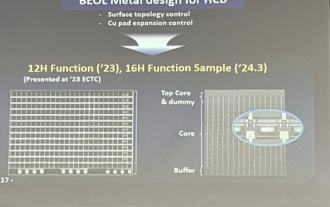
According to the report, Samsung Electronics executive Dae Woo Kim said that at the 2024 Korean Microelectronics and Packaging Society Annual Meeting, Samsung Electronics will complete the verification of the 16-layer hybrid bonding HBM memory technology. It is reported that this technology has passed technical verification. The report also stated that this technical verification will lay the foundation for the development of the memory market in the next few years. DaeWooKim said that Samsung Electronics has successfully manufactured a 16-layer stacked HBM3 memory based on hybrid bonding technology. The memory sample works normally. In the future, the 16-layer stacked hybrid bonding technology will be used for mass production of HBM4 memory. ▲Image source TheElec, same as below. Compared with the existing bonding process, hybrid bonding does not need to add bumps between DRAM memory layers, but directly connects the upper and lower layers copper to copper.
 Intel explains in detail the Intel 3 process: applying more EUV lithography, increasing the frequency of the same power consumption by up to 18%
Jun 19, 2024 pm 10:53 PM
Intel explains in detail the Intel 3 process: applying more EUV lithography, increasing the frequency of the same power consumption by up to 18%
Jun 19, 2024 pm 10:53 PM
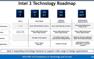
According to news from this site on June 19, as part of the 2024 IEEEVLSI seminar activities, Intel recently introduced the technical details of the Intel3 process node on its official website. Intel's latest generation of FinFET transistor technology is Intel's latest generation of FinFET transistor technology. Compared with Intel4, it has added steps to use EUV. It will also be a node family that provides foundry services for a long time, including basic Intel3 and three variant nodes. Among them, Intel3-E natively supports 1.2V high voltage, which is suitable for the manufacturing of analog modules; while the future Intel3-PT will further improve the overall performance and support finer 9μm pitch TSV and hybrid bonding. Intel claims that as its
 Samsung Electronics reiterates that the SF1.4 process is expected to be mass-produced in 2027 and plans to enter the field of co-packaging optics
Jun 13, 2024 pm 05:10 PM
Samsung Electronics reiterates that the SF1.4 process is expected to be mass-produced in 2027 and plans to enter the field of co-packaging optics
Jun 13, 2024 pm 05:10 PM
This site reported on June 13 that Samsung Electronics reiterated at the Samsung Foundry Forum 2024 North America held on June 12, local time, that its SF1.4 process is expected to be mass-produced in 2027, countering previous media rumors. Samsung said its 1.4nm process preparations are progressing smoothly and it is expected to reach mass production milestones in both performance and yield in 2027. In addition, Samsung Electronics is actively researching advanced logic process technology in the post-1.4nm era through innovations in materials and structures to realize Samsung's commitment to continuously surpass Moore's Law. Samsung Electronics simultaneously confirmed that it still plans to mass-produce the second-generation 3nm process SF3 in the second half of 2024. In the more traditional FinFET transistor segment, Samsung Electronics plans to launch S
 Samsung introduces BM1743 data center-grade SSD: equipped with v7 QLC V-NAND and supports PCIe 5.0
Jun 18, 2024 pm 04:15 PM
Samsung introduces BM1743 data center-grade SSD: equipped with v7 QLC V-NAND and supports PCIe 5.0
Jun 18, 2024 pm 04:15 PM
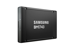
According to news from this website on June 18, Samsung Semiconductor recently introduced its next-generation data center-grade solid-state drive BM1743 equipped with its latest QLC flash memory (v7) on its technology blog. ▲Samsung QLC data center-grade solid-state drive BM1743 According to TrendForce in April, in the field of QLC data center-grade solid-state drives, only Samsung and Solidigm, a subsidiary of SK Hynix, had passed the enterprise customer verification at that time. Compared with the previous generation v5QLCV-NAND (note on this site: Samsung v6V-NAND does not have QLC products), Samsung v7QLCV-NAND flash memory has almost doubled the number of stacking layers, and the storage density has also been greatly improved. At the same time, the smoothness of v7QLCV-NAND
 It is reported that Intel CEO Pat Gelsinger will deliver a plenary speech at ISSCC for the first time next year to introduce foundry progress.
Aug 10, 2024 am 07:42 AM
It is reported that Intel CEO Pat Gelsinger will deliver a plenary speech at ISSCC for the first time next year to introduce foundry progress.
Aug 10, 2024 am 07:42 AM
According to news from this website on August 9, Korean media "Chosun Ilbo" reported that Intel CEO Pat Kissinger will attend the next IEEEISSCC International Solid-State Circuits Conference to be held in San Francisco from February 16th to 20th, 2025 local time. , and will deliver a keynote speech at the ISSCC plenary session for the first time. Note from this site: Speakers at the ISSCC2024 plenary session include Zhang Xiaoqiang, deputy co-chief operating officer of TSMC, etc.; at ISSCC2023, AMD CEO Su Zifeng, imec Chief Strategy Officer JoDeBoeck, etc. delivered plenary speeches. According to reports, Intel’s plenary speakers mainly introduce CPU-related technologies at the ISSCC conference, but Pat Kissinger’s speech to be released next year will focus on Intel’s I
 It is reported that Samsung Electronics V9 QLC NAND flash memory has not yet received mass production-ready license, affecting Pyeongtaek P4 factory planning
Jul 31, 2024 pm 08:38 PM
It is reported that Samsung Electronics V9 QLC NAND flash memory has not yet received mass production-ready license, affecting Pyeongtaek P4 factory planning
Jul 31, 2024 pm 08:38 PM
According to news from this site on July 31, Korean media ZDNetKorea reported that the QLC version of Samsung Electronics’ V9NAND flash memory has not yet received a mass production license, which has affected the production line construction planning of the Pyeongtaek P4 factory. Samsung Electronics announced in April this year that the 1Tb capacity TLC version of its V9NAND flash memory has achieved mass production, and the corresponding QLC version will enter mass production in the second half of this year. However, until now, Samsung Electronics has not issued a PRA (this site's note: should refer to Production Readiness Approval) mass production-ready license for V9QLCNAND flash memory. QLC flash memory with higher capacity and lower cost is currently the hot spot for AI inference server storage needs. The future of star products is unclear, making the three
 Samsung Electronics announced the list of partner companies in 2024: adding Tianma and CSOT India subsidiaries
Jul 03, 2024 pm 05:38 PM
Samsung Electronics announced the list of partner companies in 2024: adding Tianma and CSOT India subsidiaries
Jul 03, 2024 pm 05:38 PM
News from this website on July 3, according to thelec report, Samsung Electronics announced the list of partner companies in 2024. This list accounts for more than 80% of Samsung Electronics’ parts procurement, with a total of 113 companies, including 11 new companies, and another 11 companies were eliminated. In this list, companies such as Tianma Microelectronics Co., Ltd. have been added, and the Indian Panel Optodisplay Technology company has also been included. This company is the Indian subsidiary of China Star Optoelectronics (CSOT). But even if a company is no longer included in the list for a given year, this does not mean that the company's trading relationship with Samsung Electronics will immediately end. For example, last year was not included
