
 Technology peripherals
It Industry
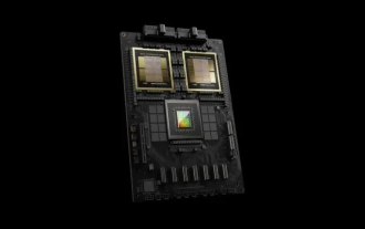
Affected by the release of 6-inch wafer production capacity and the slowdown in demand for electric vehicles, the silicon carbide market will start a price war
Technology peripherals
It Industry
Affected by the release of 6-inch wafer production capacity and the slowdown in demand for electric vehicles, the silicon carbide market will start a price war
Affected by the release of 6-inch wafer production capacity and the slowdown in demand for electric vehicles, the silicon carbide market will start a price war

According to news from this site on May 31, TrendForce released a blog post today, stating that a price war in the silicon carbide (SiC) market is about to begin. The agency investigated a number of manufacturers in the supply chain and generally believes that the price of silicon carbide wafers is on a downward trend.

The reference address is attached to this site
- A Price War in SiC Wafer Sector seems to Start
The above is the detailed content of Affected by the release of 6-inch wafer production capacity and the slowdown in demand for electric vehicles, the silicon carbide market will start a price war. For more information, please follow other related articles on the PHP Chinese website!

Hot AI Tools

Undresser.AI Undress
AI-powered app for creating realistic nude photos

AI Clothes Remover
Online AI tool for removing clothes from photos.

Undress AI Tool
Undress images for free

Clothoff.io
AI clothes remover

Video Face Swap
Swap faces in any video effortlessly with our completely free AI face swap tool!

Hot Article
Hot Tools

Notepad++7.3.1
Easy-to-use and free code editor

SublimeText3 Chinese version
Chinese version, very easy to use

Zend Studio 13.0.1
Powerful PHP integrated development environment

Dreamweaver CS6
Visual web development tools

SublimeText3 Mac version
God-level code editing software (SublimeText3)
Hot Topics


 Innolux plans to mass-produce fan-out panel-level semiconductor packaging technology by the end of the year
Aug 07, 2024 pm 06:18 PM
Innolux plans to mass-produce fan-out panel-level semiconductor packaging technology by the end of the year
Aug 07, 2024 pm 06:18 PM
According to news from this site on August 6, Yang Zhuxiang, general manager of Innolux Corporation, said yesterday (August 5) that the company is actively deploying and promoting semiconductor fan-out panel-level packaging (FOPLP) and is expected to mass-produce ChipFirst before the end of this year. The contribution of process technology to revenue will be apparent in the first quarter of next year. Fenye Innolux stated that it is expected to mass-produce the redistribution layer (RDLFirst) process technology for mid-to-high-end products in the next 1-2 years, and will work with partners to develop the most technically difficult glass drilling (TGV) process, which will take another 2-3 years. It can be put into mass production within a year. Yang Zhuxiang said that Innolux’s FOPLP technology is “ready for mass production” and will enter the market with low-end and mid-range products.
 TrendForce: Nvidia's Blackwell platform products drive TSMC's CoWoS production capacity to increase by 150% this year
Apr 17, 2024 pm 08:00 PM
TrendForce: Nvidia's Blackwell platform products drive TSMC's CoWoS production capacity to increase by 150% this year
Apr 17, 2024 pm 08:00 PM
According to news from this site on April 17, TrendForce recently released a report, believing that demand for Nvidia's new Blackwell platform products is bullish, and is expected to drive TSMC's total CoWoS packaging production capacity to increase by more than 150% in 2024. NVIDIA Blackwell's new platform products include B-series GPUs and GB200 accelerator cards integrating NVIDIA's own GraceArm CPU. TrendForce confirms that the supply chain is currently very optimistic about GB200. It is estimated that shipments in 2025 are expected to exceed one million units, accounting for 40-50% of Nvidia's high-end GPUs. Nvidia plans to deliver products such as GB200 and B100 in the second half of the year, but upstream wafer packaging must further adopt more complex products.
 SK hynix's innovative semiconductor CMP polishing pad technology enables sustainable use
Dec 28, 2023 pm 11:04 PM
SK hynix's innovative semiconductor CMP polishing pad technology enables sustainable use
Dec 28, 2023 pm 11:04 PM
According to news from this website on December 27, according to Korean media ETNews, SK Hynix has recently developed reusable CMP polishing pad technology, which can not only reduce costs, but also enhance ESG (environmental, social, governance) management. SK Hynix said that they will first deploy reusable CMP polishing pads in low-risk processes and gradually expand their application scope. Note: CMP technology is to make the surface of the material to be polished under the combined action of chemicals and mechanics. A process to achieve the required flatness. The chemical components in the polishing fluid react chemically with the material surface to form a softened layer that is easy to polish. The polishing pad and abrasive particles in the polishing fluid physically and mechanically polish the material surface to remove the softened layer. Source: Dinglong shares in CM
 Sony Group: Its semiconductor factories concealed emissions of harmful substances
Jul 12, 2024 pm 02:09 PM
Sony Group: Its semiconductor factories concealed emissions of harmful substances
Jul 12, 2024 pm 02:09 PM
According to reports from this website on July 8, based on reports from Nikkei and Japan's "Jiji News Agency", on the 8th (today) local time, Sony Semiconductor Manufacturing Company, a semiconductor manufacturer under the Sony Group, announced that the company had discharged harmful chemicals outside the factory. , and no notification was made. The company said this was due to an input error and an imperfect confirmation system. In fiscal years 2021 and 2022, the camera image sensor factory located in Kikuyo Town, Kumamoto Prefecture, incorrectly reported its emissions of chemical substances as 0. The actual situation was that there were emissions of "waste without harmless treatment." The plant emits hydrogen fluoride, which is commonly used in semiconductor processing and cleaning. Note from this site: Hydrogen fluoride is harmful to the human body and can cause respiratory diseases and even life-threatening effects when inhaled. sony half
 What is the main difference between semiconductor read-only memory and semiconductor random access memory?
Dec 09, 2020 am 09:57 AM
What is the main difference between semiconductor read-only memory and semiconductor random access memory?
Dec 09, 2020 am 09:57 AM
The main difference is that semiconductor read-only memory ROM can store information permanently, while semiconductor random access memory RAM will lose information when the power is turned off. The characteristic of ROM is that it can only read information but cannot write information; and the content will not be lost after power is turned off, and it will automatically restore after powering on. The characteristic of RAM is its fast reading and writing speed. Its biggest disadvantage is that the contents inside it disappear immediately after the power is turned off.
 Samsung plans to invest 10 trillion won in semiconductor equipment and purchase ASML EUV lithography machines in large quantities
Nov 15, 2023 pm 12:33 PM
Samsung plans to invest 10 trillion won in semiconductor equipment and purchase ASML EUV lithography machines in large quantities
Nov 15, 2023 pm 12:33 PM
Samsung plans to increase the import of more ASML extreme ultraviolet (EUV) lithography equipment, according to a report from South Korea's Electronic News Today. Although the confidentiality clause in the contract did not disclose specific details, according to securities market news, this agreement will allow ASML to A total of 50 sets of equipment will be provided within five years. The unit price of each equipment is approximately 200 billion won (approximately 1.102 billion yuan), and the total value can reach 10 trillion won (approximately 55.1 billion yuan). It is currently unclear what the contract The product is an existing EUV lithography equipment or a next-generation "HighNAEUV" lithography equipment. However, the biggest problem with current EUV lithography equipment is limited output. According to officials, it is "more complex than satellite components" and can only be produced in very limited quantities each year. according to
 It is reported that Pioneer International Semiconductor acquires AUO's Singapore factory to build an advanced 12-inch automotive chip wafer fab
Oct 31, 2023 pm 12:37 PM
It is reported that Pioneer International Semiconductor acquires AUO's Singapore factory to build an advanced 12-inch automotive chip wafer fab
Oct 31, 2023 pm 12:37 PM
According to news from this site on October 31, the Economic Daily learned from industry insiders that Pioneer International Semiconductor/World Advanced (VIS) is currently negotiating with AUO's Singapore factory to acquire the land and equipment held by the latter and use it to Construction of the first 12-inch wafer fab. Source: AUO’s official website Pioneer International Semiconductor plans to invest US$2 billion (approximately RMB 14.64 billion) to produce chips, mainly for the automotive field. According to reports, Pioneer International Semiconductor will hold a relevant meeting on November 7. AUO plans to hold a relevant meeting on October 31. The two companies have not yet issued official comments on the relevant rumors. Reports indicate that AUO plans to gradually withdraw its development focus in Singapore from manufacturing to establishing a regional service center. This Singapore factory was established in 201
 It can reduce the use of expensive EUV lithography. Merck of Germany says DSA self-assembly technology will be commercially available within ten years.
Feb 05, 2024 pm 02:40 PM
It can reduce the use of expensive EUV lithography. Merck of Germany says DSA self-assembly technology will be commercially available within ten years.
Feb 05, 2024 pm 02:40 PM
According to news from this website on February 5, Anand Nambier, senior vice president of Merck of Germany, said at a press conference recently that DSA self-assembly technology will be commercialized in the next ten years, which can reduce the number of expensive EUV patterning and become an existing photolithography A great addition to the technology. Note from this site: DSA stands for Directedself-assembly, which uses the surface characteristics of block copolymers to realize the automatic construction of periodic patterns, and then induces them to eventually form the desired pattern with controllable direction. It is generally believed that DSA is not suitable for use as an independent patterning technology, but is combined with other patterning technologies (such as traditional photolithography) to produce high-precision semiconductors. ▲AnandNambier at the press conference. Picture source T
