 Technology peripherals
 It Industry
 Micron plans to set up more semiconductor chip units in India
Micron plans to set up more semiconductor chip units in India
News from this site on September 18, according to "Mint", India's Minister of Electronics and Information Technology Rajeev Chandrasekhar said that in addition to the proposed manufacturing unit, Micron also intends to establish multiple semiconductor assembly and packaging units in India. Micron will We are optimistic about the Indian market in the long term.
The minister said that Micron’s investment in India has prompted a change of attitude among those on the sidelines; therefore, it is in the government’s interest to ensure that the company’s first factory becomes operational as soon as possible
Micron CEO Sang Jai Mehrotra said at Semicon India 2023 in July this year that the semiconductor and packaging giant will begin the next phase of expansion after 2025.
The company has previously announced an investment of US$800 million (approximately RMB 5.832 billion) to establish a semiconductor assembly, test, marking and packaging (ATMP) factory in Sanad, Gujarat, India. Indian officials said that as the first factory becomes operational, more similar facilities will appear.
Micron's first successful investment in India will bring two major benefits. First, it will provide guidance to other companies and investors, encouraging them to invest in Doleira or elsewhere. Secondly, these companies coming to India will see an increase in value and have the opportunity to expand further
He also mentioned: "We have created a policy framework to attract a globally important company, and they will Starting with packaging, it is expected to enter the semiconductor manufacturing field in the next four to five years. The Indian government is talking to all entities in the semiconductor market, and the level of participation in discussions has increased significantly compared to entities that were less focused on India before.”
He added that wafer fabs usually appear in large numbers in a certain area, including packaging plants. Taking Malaysia and Japan as examples, he said: "If you look at the history of the development of wafer fabs and packaging fabs anywhere in the world, you will find that they all started from a small scale. Unless the local environment or government policy changes An extremely bad change, otherwise they will all expand to large-scale complexes with multiple factories, multiple fabs, and multiple packaging plants.”
Currently, the Indian government has provided approximately US$1.95 billion to Micron (currently approximately US$14.216 billion). billion RMB) of financial assistance, and the current total investment in the project has reached US$2.75 billion (currently approximately RMB 20.047 billion). Construction of the facility is expected to begin this year, with the first phase expected to be operational by the end of 2024, and India expects its first locally produced chips to be available in December 2024.
Advertising statement: The external jump links (including but not limited to hyperlinks, QR codes, passwords, etc.) contained in the article are used to convey more information and save selection time. The results are for reference only. All articles on the site contain this statement.
The above is the detailed content of Micron plans to set up more semiconductor chip units in India. For more information, please follow other related articles on the PHP Chinese website!

Hot AI Tools

Undresser.AI Undress
AI-powered app for creating realistic nude photos

AI Clothes Remover
Online AI tool for removing clothes from photos.

Undress AI Tool
Undress images for free

Clothoff.io
AI clothes remover

Video Face Swap
Swap faces in any video effortlessly with our completely free AI face swap tool!

Hot Article

Hot Tools

Notepad++7.3.1
Easy-to-use and free code editor

SublimeText3 Chinese version
Chinese version, very easy to use

Zend Studio 13.0.1
Powerful PHP integrated development environment

Dreamweaver CS6
Visual web development tools

SublimeText3 Mac version
God-level code editing software (SublimeText3)

Hot Topics
 1664
1664
 14
14
 1422
1422
 52
52
 1316
1316
 25
25
 1268
1268
 29
29
 1242
1242
 24
24
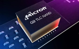
 Industry's highest transfer rate of 3.6GB/s, Micron announces mass production of ninth-generation 276-layer TLC NAND flash memory
Jul 31, 2024 am 08:05 AM
According to news from this site on July 30, Micron announced today (local time) that its ninth generation (site note: 276 layers) 3DTLC NAND flash memory will be mass-produced and shipped. Micron said that its G9NAND has the industry's highest I/O transfer rate of 3.6GB/s (i.e. 3600MT/s flash memory interface rate), which is 50% higher than the existing competing products of 2400MT/s, and can better meet the needs of data-intensive workloads. High throughput requirements. At the same time, Micron's G9NAND is 99% and 88% higher than other solutions on the market in terms of write bandwidth and read bandwidth respectively. This NAND particle-level advantage will bring performance and energy efficiency to solid-state drives and embedded storage solutions. improvement. In addition, like previous generations of Micron NAND flash memory, Micron 276
 India production is not going well, Apple moves some iPhone production capacity back to China
Jul 24, 2024 pm 12:24 PM
On July 23, some media reported that Apple has implemented a “risk aversion” and supply chain diversification strategy in recent years, especially its attempt to shift production orders to India. However, this transformation process has not been smooth sailing. Last year, Indian factories suffered setbacks when assembling iPhone 15. The products were returned due to quality problems and had to take price reduction measures, forcing Apple CEO Tim Cook to personally go to China to adjust the supply chain layout. In view of the above experience, Apple has quickly adjusted its strategy this year, and some production capacity has returned to mainland China. Industry giants such as BYD and Luxshare Precision have been included in the iPhone 16 supply chain system and have become Apple's new partners. The birth of Foxconn in Sriperumbudur, India
 Micron: HBM memory consumes 3 times the wafer volume, and production capacity is basically booked for next year
Mar 22, 2024 pm 08:16 PM
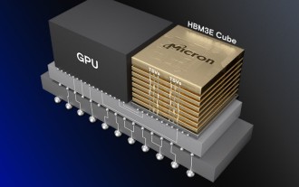
This site reported on March 21 that Micron held a conference call after releasing its quarterly financial report. At the conference, Micron CEO Sanjay Mehrotra said that compared to traditional memory, HBM consumes significantly more wafers. Micron said that when producing the same capacity at the same node, the current most advanced HBM3E memory consumes three times more wafers than standard DDR5, and it is expected that as performance improves and packaging complexity intensifies, in the future HBM4 This ratio will further increase. Referring to previous reports on this site, this high ratio is partly due to HBM’s low yield rate. HBM memory is stacked with multi-layer DRAM memory TSV connections. A problem with one layer means that the entire
 Innolux plans to mass-produce fan-out panel-level semiconductor packaging technology by the end of the year
Aug 07, 2024 pm 06:18 PM
According to news from this site on August 6, Yang Zhuxiang, general manager of Innolux Corporation, said yesterday (August 5) that the company is actively deploying and promoting semiconductor fan-out panel-level packaging (FOPLP) and is expected to mass-produce ChipFirst before the end of this year. The contribution of process technology to revenue will be apparent in the first quarter of next year. Fenye Innolux stated that it is expected to mass-produce the redistribution layer (RDLFirst) process technology for mid-to-high-end products in the next 1-2 years, and will work with partners to develop the most technically difficult glass drilling (TGV) process, which will take another 2-3 years. It can be put into mass production within a year. Yang Zhuxiang said that Innolux’s FOPLP technology is “ready for mass production” and will enter the market with low-end and mid-range products.
 TrendForce: Nvidia's Blackwell platform products drive TSMC's CoWoS production capacity to increase by 150% this year
Apr 17, 2024 pm 08:00 PM
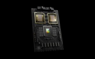
According to news from this site on April 17, TrendForce recently released a report, believing that demand for Nvidia's new Blackwell platform products is bullish, and is expected to drive TSMC's total CoWoS packaging production capacity to increase by more than 150% in 2024. NVIDIA Blackwell's new platform products include B-series GPUs and GB200 accelerator cards integrating NVIDIA's own GraceArm CPU. TrendForce confirms that the supply chain is currently very optimistic about GB200. It is estimated that shipments in 2025 are expected to exceed one million units, accounting for 40-50% of Nvidia's high-end GPUs. Nvidia plans to deliver products such as GB200 and B100 in the second half of the year, but upstream wafer packaging must further adopt more complex products.
 SK hynix's innovative semiconductor CMP polishing pad technology enables sustainable use
Dec 28, 2023 pm 11:04 PM
According to news from this website on December 27, according to Korean media ETNews, SK Hynix has recently developed reusable CMP polishing pad technology, which can not only reduce costs, but also enhance ESG (environmental, social, governance) management. SK Hynix said that they will first deploy reusable CMP polishing pads in low-risk processes and gradually expand their application scope. Note: CMP technology is to make the surface of the material to be polished under the combined action of chemicals and mechanics. A process to achieve the required flatness. The chemical components in the polishing fluid react chemically with the material surface to form a softened layer that is easy to polish. The polishing pad and abrasive particles in the polishing fluid physically and mechanically polish the material surface to remove the softened layer. Source: Dinglong shares in CM
 Analyst: Micron's non-volatile NVDRAM memory has many highlights, but is unlikely to be commercialized
Jan 30, 2024 pm 06:30 PM
According to news from this site on January 29, Micron disclosed its 32Gb3DNVDRAM (non-volatile DRAM) research and development results at the IEEEIEDM conference in late 2023. However, according to information obtained by foreign media Blocks&Files from two industry analysts interviewed, this breakthrough new memory is basically unlikely to be commercialized and mass-produced, but the technological progress it demonstrates is expected to appear in future memory products. . Micron's NVDRAM memory is based on the principle of ferroelectricity (note from this site: it has spontaneous polarization, and the polarization direction can be reversed under an external electric field). It can achieve high performance close to DRAM while having non-volatility similar to NAND flash memory. Durable and low latency. This new type of memory uses double-layer 3D stacking and has a capacity of 32Gb.
 Sony Group: Its semiconductor factories concealed emissions of harmful substances
Jul 12, 2024 pm 02:09 PM
According to reports from this website on July 8, based on reports from Nikkei and Japan's "Jiji News Agency", on the 8th (today) local time, Sony Semiconductor Manufacturing Company, a semiconductor manufacturer under the Sony Group, announced that the company had discharged harmful chemicals outside the factory. , and no notification was made. The company said this was due to an input error and an imperfect confirmation system. In fiscal years 2021 and 2022, the camera image sensor factory located in Kikuyo Town, Kumamoto Prefecture, incorrectly reported its emissions of chemical substances as 0. The actual situation was that there were emissions of "waste without harmless treatment." The plant emits hydrogen fluoride, which is commonly used in semiconductor processing and cleaning. Note from this site: Hydrogen fluoride is harmful to the human body and can cause respiratory diseases and even life-threatening effects when inhaled. sony half


