

Can Tesla supercomputing chip surpass GPGPU?

Author: Chen Wei, Ph.D., storage and computing integration/GPU architecture and AI expert, senior professional title. Zhongguancun Cloud Computing Industry Alliance, expert of China Optical Engineering Society, member of International Computer Federation (ACM), professional member of China Computer Federation (CCF). He used to be the chief scientist of an AI company and the head of 3D NAND design of a major memory chip manufacturer. His main achievements include the first domestic high-power reconfigurable storage and computing processor product architecture (has completed prototype internal testing in a major Internet manufacturer), the first medical Domain-specific AI processor (already applied), the first RISC-V/x86/ARM platform-compatible AI acceleration compiler (already applied in cooperation with Alibaba Pingtouge/Xinlai), China's first 3D NAND chip architecture and design The team was established (benchmarked with Samsung) and the first embedded flash memory compiler in China (benchmarked with TSMC and has been applied at the platform level).
On the last day of September 2022, Tesla’s Artificial Intelligence Day, Tesla’s “Optimus Prime” robot officially debuted. According to Tesla engineers, Artificial Intelligence Day 2022 is the first time that Tesla robots have been "released" without any external support. "He walked dignifiedly and greeted the audience in a general direction. Except for the slightly sluggish movements, everything else is very natural.
1 Does the power of Tesla robots lie in its “inner core”?
Tesla shows off video of robots "working" around the office. A robot named Optimus Prime carried items, watered plants, and even worked autonomously in a factory for a while. "Our goal is to build useful humanoid robots as quickly as possible," Tesla said, adding that their goal is to make the robots less than $20,000, or cheaper than Tesla's electric cars.
The reason why Tesla robots are so powerful is not only Tesla’s own accumulation of AI technology, but also mainly due to Tesla’s strong self-developed AI chips. This AI chip is not a traditional CPU, let alone a GPU. It is a form more suitable for complex AI calculations.
Comparison of D1 processor and other autonomous driving/robotics processors

1.1 Based on the data flow near-memory architecture to create a general-purpose AI chip that surpasses the GPU
The reason why Tesla builds its own chip is that the GPU is not specifically designed to handle deep learning training, which makes GPUs are relatively inefficient in computing tasks. The goal of Tesla and Dojo (Dojo is both the name of the training module and the name of the kernel architecture) is to "achieve the best AI training performance. Enable larger and more complex neural network models to achieve high energy efficiency and cost-effectiveness." Computing." Tesla's standard is to build a computer that is better at artificial intelligence computing than any other computer so that they don't need to use a GPU in the future.
A key point in building supercomputers is how to scale computing power while maintaining high bandwidth (difficult) and low latency (very difficult). The solution given by Tesla is a distributed 2D architecture (planar) composed of powerful chips and a unique grid structure, or a data flow near-memory computing architecture.
Hierarchical division of Tesla computing units

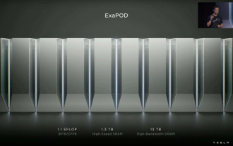
According to the hierarchy, every 354 Dojo cores form a D1 chip, and every 25 chips form a training module. The final 120 training modules form a set of ExaPOD computing clusters, with a total of 3,000 D1 chips.
A Tesla Dojo chip training module can achieve the performance of 6 groups of GPU servers, but the cost is less than a single group of GPU servers. The computing power of a single Dojo server even reached 54PFLOPS. Just 4 Dojo cabinets can replace 72 GPU racks consisting of 4,000 GPUs. Dojo reduces AI computing (training) work that normally takes months to 1 week. This kind of "big computing power can produce miracles" is in line with Tesla's autonomous driving style. Obviously, the chip will also greatly accelerate the progress of Tesla's AI technology.
Of course, this chip module has not yet reached the level of "perfection". Although it adopts the idea of data stream near-memory computing, its computing power and energy efficiency ratio does not exceed that of the GPU. A single server consumes huge power, with the current reaching 2000A, and requires a specially customized power supply. The Tesla D1 chip is already the structural limit of the near-memory computing architecture. If Tesla adopts "in-memory computing" or "in-memory logic" architecture, perhaps the chip performance or energy efficiency ratio will be greatly improved.

The Tesla Dojo chip server consists of 12 Dojo training modules (2 layers, 6 per layer)
1.2 Tesla’s Dojo architecture design philosophy
The Dojo core is an 8-way decoding core with high throughput and 4-way matrix calculation unit (8x8) and 1.25 MB. Local SRAM. However, the size of the Dojo core is not large. In comparison, Fujitsu's A64FX occupies more than twice the area on the same process node.
Through the structure of the Dojo core, we can see Tesla’s design philosophy on general AI processors:
- Area reduction: Tesla integrates a large number of computing cores into the chip to maximize the throughput of AI computing. Therefore, it is necessary to make the area of a single core as small as possible while ensuring computing power, which is a better compromise for supercomputing. The contradiction between computing power stacking and delay in the system.
- Cache and latency reduction: In order to maximize its area computing efficiency, the Dojo core runs at a relatively conservative 2 GHz (conservative clock circuits tend to occupy less area), using only basic branch predictor and small instruction cache, in such a streamlined architecture that only retains necessary components. The remaining area is left as much as possible to the vector calculation and matrix calculation units. Of course, if the kernel program has a large code footprint or has many branches, this strategy may sacrifice some performance.
- Feature reduction: Further reduce power and area usage by cutting out processor functions that are not necessary to run internal calculations. Dojo core does not perform data-side caching, does not support virtual memory, and does not support precise exceptions.
For Tesla and Musk, Dojo is not only shaped and laid out like a dojo, but its design philosophy is also closely related to the spirit of the dojo, fully embodying "less is more" "Multiple" processor design aesthetics.
2 Is the core of D1 a RISC-V architecture?
Let’s first take a look at the structure and characteristics of each Dojo.
Each Dojo core is a processor with vector calculation/matrix calculation capabilities, and has complete instruction fetching, decoding, and execution components. Dojo core has a CPU-like style that seems to be more adaptable to different algorithms and branching code than GPU. The instruction set of D1 is similar to RISC-V. The processor runs at 2GHz and has four sets of 8x8 matrix multiplication calculation units. It also has a set of custom vector instructions focused on accelerating AI calculations.
Those who are familiar with the RISC-V field can probably tell that the color scheme of Tesla’s Dojo architecture diagram seems to pay tribute to Berkeley’s BOOM processor architecture diagram, with yellow at the top, green at the bottom purple.

##Comparison between Tesla Dojo core and Berkeley BOOM/IBM Cell core
2.1 D1 core overall architecture
D1 core structure (the blue part is the added/modified details)
Judging from the current architecture diagram, the Dojo core consists of 4 parts: front-end, execution unit, SRAM and NoC routing. It has fewer control components than both CPU and GPU. It has a CPU-like AGU and an idea similar to GPU tensors. The matrix computing unit of the core (Tensor core).
The core structure of Dojo is more streamlined than BOOM. It does not have components such as Rename to improve the utilization of execution components, and it is also difficult to support virtual memory. However, the advantage of this design is that it reduces the area occupied by the control part and can allocate more area on the chip to the calculation execution unit. Each Dojo core provides 1.024TFLOPS of computing power. It can be seen that almost all the computing power of each is provided by the matrix computing unit. Therefore, the matrix computing unit and SRAM jointly determine the computing energy efficiency ratio of the D1 processor.
Main parameters of Dojo core

- Branch prediction: Compared with SIMT architectures such as GPUs, the Dojo core does not have a SIMT stack core to allocate multi-threaded branch tasks. But Dojo core has BTB (branch target buffer), so D1 can improve performance through simple branch prediction.
BTB saves the address of the successful branch instruction and its branch target address in a buffer. The buffer is identified by the address of the branch instruction. The performance penalty of branches in pipelined processors can be reduced by predicting the path of the branch and caching the information used by the branch. - Instruction cache: The smaller L1 instruction cache is directly connected to the SRAM in the core to obtain computing instructions.
- Instruction fetch: Each Dojo kernel has a 32B instruction fetch window, which can accommodate up to 8 instructions.
- Decoding: An 8-way decoder can handle two threads per cycle. The decoding phase obtains instructions from the fetch buffer and decodes them, and allocates necessary execution resources according to the requirements of each instruction.
- Thread scheduling: After the wider 8-way decoding, there is the vector scheduler (Scheduler) and register file (Register File). It seems that there is no mask judgment for branch aggregation here, and the actual branch execution efficiency may be slightly lower than that of the GPU. Hopefully Tesla has a powerful compiler.
- Execution unit: with 2-way ALU and 2-way AGU, as well as 512-bit SIMD and matrix calculation units for vector/matrix calculations (performing 512-bit vector calculations and 4-way 8x8 matrices respectively multiplication). The matrix computing unit is the main computing power of the D1 chip. (Introduced in detail in the next section)
- ALU and AGU are mainly responsible for a small amount of logical calculations other than matrix calculations. The AGU is the address generation unit, which is mainly used to generate the addresses required to operate the SRAM and access the addresses of other cores. By running the address computation in parallel with the rest of the CPU.
When an ordinary CPU performs various operations, it needs to calculate the memory address required to retrieve data from memory (or SRAM). For example, the memory location of an array element must be calculated before the CPU core can get the data from the actual memory location. These address generation calculations involve different integer arithmetic operations such as addition, subtraction, modulo arithmetic, or bit shifting. Calculating the memory address can compile multiple general machine instructions, or it can be executed directly through the AGU hardware circuit like Tesla Dojo. In this way, various address generation calculations can be offloaded from the ALU, reducing the number of CPU cycles required to perform AI calculations, thereby improving computing performance. - SIMD is mainly responsible for calculation of special functions such as activation and accumulation of data.
- The matrix calculation unit is the main computing component of Dojo. It is responsible for two-dimensional matrix calculations and then implements convolution, Transformer and other calculations.

Intel Nehalem architecture uses AGU to improve single-cycle address access efficiency
The connection method of the Dojo kernel is more similar to the SPE kernel connection method in IBM's Cell processor. Key similarities include:
- Neither code running on D1 or SPE has direct access to system memory, applications work primarily in local SRAM;
- If data from main memory (DDR or HBM) is required, DMA operation must be used to read it in.
- Neither D1 nor Cell's SPE supports virtual memory.
The calculation and matrix multiplication module and the storage of the kernel will be introduced below.
2.2 Computing power core matrix computing unit and on-chip storage
The core of Dojo architecture computing power enhancement is the matrix computing unit. The data interaction between the matrix computing unit and the core SRAM constitutes the main core data handling power consumption.
The corresponding patent of Tesla matrix calculation unit is as follows. The key component of this module is an 8x8 matrix-matrix multiplication unit (called a matrix calculator in the figure). The input is the data input array and the weight input array. After calculating the matrix multiplication, the output is directly accumulated. Each Dojo core includes 4-way 8x8 matrix multiplication units.

Tesla Matrix Computing Unit Patent
Since there is only one L1 cache and SRAM on the architecture diagram, it is a bold guess that Tesla has streamlined the RISC-V cache structure in order to save cache area and reduce latency. The 1.25MB SRAM block per core can provide 2x512-bit read (corresponding to the weight and data of AI calculations) and 512-bit write bandwidth for SIMD and matrix computing units, as well as 64-bit read and write capabilities for the integer register file. The main data flow of computation is from SRAM to SIMD and matrix multiplication units.
The main processing flow of the matrix calculation unit is:
Load weights from SRAM to the weight input array through the multiplexer (Mux) (Weight input array), and at the same time load data in SRAM to the data input array (Data input array).
The input data and weights are multiplied in the matrix calculator (Matrix computation Unit) (inner product or outer product?)
The multiplication calculation results are output to the output accumulator (Output accumulator) for accumulation. When calculating here, matrix calculations exceeding 8x8 can be performed by matrix division and splicing.
The accumulated output is passed into the post-processor register file for caching, and then post-processing (operations such as activation, pooling, padding, etc. can be performed).
The entire calculation process is directly controlled by the control unit (Control unit) without CPU intervention.

Data interaction between execution unit and SRAM/NoC
Dojo core The SRAM inside has very large read and write bandwidth and can load at 400 GB/sec and write at 270 GB/sec. The Dojo core instruction set has dedicated network transfer instructions, routed through the NoC, that can move data directly into or out of the SRAM memory of other cores in the D1 chip or even in the Dojo training module.
Different from ordinary SRAM, Dojo's SRAM includes a list parser engine and a gather engine. The list parsing function is one of the key features of the D1 chip. The list parsing engine can package complex transmission sequences of different data types to improve transmission efficiency.

List parsing function
In order to further reduce operation delay, area and Complexity,D1 does not support virtual memory. In a normal processor, the memory address used by the program does not directly access the physical memory address, but is converted into a physical address by the CPU using the paging structure set by the operating system.
In the D1 core, the 4-way SMT function allows explicit parallelism in calculations, simplifying the AGU and addressing calculation methods to allow Tesla to access SRAM with low enough latency. The advantage is that it avoids the delay of intermediate L1 data cache.
2.3 Dojo Instruction Set

D1 Processor Instruction Set
D1 Reference RISC-V architecture instructions are introduced, and some instructions are customized, especially those related to vector calculations.
The D1 instruction set supports 64-bit scalar instructions and 64-byte SIMD instructions, network transmission and synchronization primitives and specialized primitives related to machine learning/deep learning (such as 8x8 matrix calculations) .
In terms of network data transmission and synchronization primitives, it supports instruction primitives (Primitives) for transmitting data from local storage (SRAM) to remote storage, as well as semaphores (Semaphore) and barriers. Barrier constraints. This allows D1 to support multi-threading, and its memory operation instructions can run on multiple D1 cores.
For machine learning and deep learning, Tesla defines instructions including mathematical operations such as shuffle, transpose, and convert, as well as instructions related to stochastic rounding and padding.
2.4 Data format
The D1 core has two standard calculation formats, FP32 and FP16, and also has the BFP16 format that is more suitable for Inference. To achieve the performance improvements of mixed-precision computing, the D1 also uses the 8-bit CFP8 format for lower precision and higher throughput.
The advantage of using CFP8 is that it can save more multiplier space to achieve almost the same computing power, which is very helpful to increase the computing power density of D1.
The Dojo compiler can slide around the mantissa precision to cover a wider range and precision. Up to 16 different vector formats can be used at any given time, giving you the flexibility to increase computing power.

D1 processor data format
According to Tesla The information can be calculated using CFP8 inside the matrix multiplication unit (stored in CFP16 format).
3 Can Dojo architecture processor surpass GPU?
The D1 processor is manufactured by TSMC and uses a 7-nanometer manufacturing process. It has 50 billion transistors and a chip area of 645mm², which is smaller than Nvidia’s A100 (826 mm²) and AMD Arcturus (750 mm²).
3.1 Dojo data flow near-memory computing architecture

D1 processor structure
Each D1 processor is composed of 18 x 20 Dojo core splices. There are 354 Dojo cores available in each D1 processor. (The reason why only 354 of the 360 cores are used is for yield and per-processor core stability considerations) It is manufactured by TSMC, using a 7nm manufacturing process, with 50 billion transistors and a chip area of 645mm².
Each Dojo core has a 1.25MB SRAM as the main weight and data storage. Different Dojo cores are connected through on-chip network routing (NoC routing), and different Dojo cores perform data synchronization through complex NoC networks instead of sharing data caches. The NoC can handle 8 packets in 4 directions (southeast, northwestern) across node boundaries, 64 B/per clock cycle in each direction, i.e. one packet input and one packet output into the mesh in all four directions Each adjacent Dojo core. The NoC router can also perform a 64B bidirectional read and write to the SRAM within the core once per cycle.

Cross-processor transfer and task division within the D1 processor
Each Dojo core is a relatively complete CPU-like with matrix computing capabilities (because each core has a separate matrix computing unit and the front end is relatively small, it is called a CPU-like here). Its data flow architecture is somewhat similar. Due to SambaNova's two-dimensional data flow grid structure, data flows directly between each processing core without returning to memory.
The D1 chip runs at 2GHz and has a huge 440MB of SRAM. Tesla focuses its design on distributed SRAM in the computing grid, reducing the frequency of memory access through a large number of faster and closer on-chip storage and the transfer between on-chip storage to improve the performance of the entire system, which has obvious Features of the data flow storage and computing integrated architecture (data flow near-memory computing).
Each D1 chip has 576 bidirectional SerDes channels distributed around it and can be connected to other D1 chips with a single-side bandwidth of 4 TB/sec.
D1 processor chip main parameters

Each D1 training module is arranged in a 5x5 D1 chip array and interconnected in a two-dimensional Mesh structure. The on-chip cross-core SRAM reaches an astonishing 11GB, and of course the power consumption also reaches an astonishing 15kW. The energy efficiency ratio is 0.6TFLOPS/W@BF16/CFP8. (I hope I calculated it wrong, otherwise this energy efficiency ratio is indeed not ideal). External 32GB shared HBM memory. (HBM2e or HBM3)

Tesla D1 processor heat dissipation structure patent
Tesla uses a dedicated Power regulation module (VRM) and thermal structure to manage power consumption. There are two main purposes of power consumption management here:
Reduce unnecessary power loss and improve energy efficiency ratio.
Reduce processor module failure caused by thermal deformation.
According to Tesla’s patent, we can see that the power regulation module is perpendicular to the chip itself, which greatly reduces the area occupied by the processor plane and can be cooled through liquid cooling. Quickly balance processor temperatures.

Tesla D1 processor heat dissipation and packaging structure patent
The training module uses InFO_SoW (Silicon on Wafer) packaging to increase the interconnection density between chips. In addition to TSMC's INFO_SoW technology, this package also uses Tesla's own mechanical packaging structure to reduce the failure of the processor module.
40 I/O chips at the outer edge of each training module achieve 36 TB/s aggregate bandwidth, or 10 TB/s span bandwidth. Each layer of training modules is connected to an ultra-fast storage system: 640GB of running memory can provide more than 18TB/s of bandwidth, plus more than 1TB/s of network switching bandwidth.
The data transmission direction is parallel to the chip plane, and the power supply and liquid cooling directions are perpendicular to the chip plane. This is a very beautiful structural design, and different training modules can be interconnected. Through the three-dimensional structure, the power supply area of the chip module is saved and the distance between computing chips is reduced as much as possible.
A Dojo POD cabinet consists of two layers of computing trays and storage systems. Each level of pallet has 6 D1 training modules. A cabinet composed of 12 training modules on two floors can provide 108PFLOPS of deep learning computing power.

##Dojo module and Dojo POD cabinet
3.3 Power management and heat dissipation controlThe heat dissipation of supercomputing platforms has always been an important dimension to measure the level of supercomputing systems.
Thermal design power of D1 chip
Tesla uses a fully self-developed VRM (Voltage Regulation Module) on the Dojo POD , a single VRM can provide 52V voltage and a huge current of more than 1000A on a circuit less than the area of a 25-cent coin. The current target is 0.86A per square millimeter, with a total of 12 independent power supply phases.

Tesla’s power conditioning module
For high density In terms of chip heat dissipation, the focus is on controlling the coefficient of thermal expansion (CTE). The chip density of the Dojo system is extremely high. If the CTE is slightly out of control, it may cause structural deformation/failure, resulting in connection failure.
Tesla’s self-developed VRM has iterated 14 versions in the past 2 years, using a MEMS oscillator (MO) to sense the thermal deformation of the power regulation module, and finally Fully meets internal requirements for CTE indicators. This method of actively adjusting the power supply through MEMS technology is similar to the active adjustment method of controlling the vibration of the rocket body.
3.4 Compilation ecology of Dojo architecture processor
For AI chips such as D1, the compilation ecology is no less important than the chip itself.
On the D1 processor plane, D1 is divided into matrix computing units. The compilation tool chain is responsible for dividing tasks and configuring data storage, and performs fine-grained parallel computing in a variety of ways to reduce storage usage. The parallel methods supported by the Dojo compiler include data parallelism, model parallelism and graph parallelism. Supported storage allocation methods include distributed tensors, recalculated allocation, and split-fill. The compiler itself can handle dynamic control flow commonly used in various CPUs, including loops and graph optimization algorithms. With the Dojo compiler, users can treat Dojo large-scale distributed systems as an accelerator for overall design and training. The top layer of the entire software ecosystem is based on PyTorch, the bottom layer is based on Dojo driver, and the Dojo compiler and LLVM are used in the middle to form the compilation layer. After adding LLVM here, Tesla can better utilize the various compilation ecosystems already on LLVM for compilation optimization. 
Tesla Dojo Compiler
4 Conclusion
Through Tesla AI Day, we saw the true form of the Tesla robot and learned more about its powerful "inner core".
Tesla’s Dojo core is different from previous CPU and GPU architectures. It can be said to be a streamlined GPU that combines the characteristics of the CPU. I believe it will also be compiled with the CPU. There is a big difference with GPU. In order to increase computing density, Tesla has made extremely streamlined optimizations and provided an actively adjusted power management mechanism.
The Tesla Dojo architecture is not only called a dojo, but its design is also based on simplicity and less as more. Will this architecture become another typical form of computing chip architecture after CPU and GPU? let us wait and see.
The above is the detailed content of Can Tesla supercomputing chip surpass GPGPU?. For more information, please follow other related articles on the PHP Chinese website!

Hot AI Tools

Undresser.AI Undress
AI-powered app for creating realistic nude photos

AI Clothes Remover
Online AI tool for removing clothes from photos.

Undress AI Tool
Undress images for free

Clothoff.io
AI clothes remover

Video Face Swap
Swap faces in any video effortlessly with our completely free AI face swap tool!

Hot Article
Hot Tools

Notepad++7.3.1
Easy-to-use and free code editor

SublimeText3 Chinese version
Chinese version, very easy to use

Zend Studio 13.0.1
Powerful PHP integrated development environment

Dreamweaver CS6
Visual web development tools

SublimeText3 Mac version
God-level code editing software (SublimeText3)
Hot Topics
 1664
1664
 14
1423
52
1321
25
1269
29
1249
24
14
1423
52
1321
25
1269
29
1249
24

 Tesla Dojo supercomputing debut, Musk: The computing power of AI training by the end of the year will be approximately equal to 8,000 NVIDIA H100 GPUs
Jul 24, 2024 am 10:38 AM
Tesla Dojo supercomputing debut, Musk: The computing power of AI training by the end of the year will be approximately equal to 8,000 NVIDIA H100 GPUs
Jul 24, 2024 am 10:38 AM
According to news from this website on July 24, Tesla CEO Elon Musk (Elon Musk) stated in today’s earnings conference call that the company is about to complete the largest artificial intelligence training cluster to date, which will be equipped with 2 Thousands of NVIDIA H100 GPUs. Musk also told investors on the company's earnings call that Tesla would work on developing its Dojo supercomputer because GPUs from Nvidia are expensive. This site translated part of Musk's speech as follows: The road to competing with NVIDIA through Dojo is difficult, but I think we have no choice. We are now over-reliant on NVIDIA. From NVIDIA's perspective, they will inevitably increase the price of GPUs to a level that the market can bear, but
 Tesla finally takes action! Will self-driving taxis be unveiled soon? !
Apr 08, 2024 pm 05:49 PM
Tesla finally takes action! Will self-driving taxis be unveiled soon? !
Apr 08, 2024 pm 05:49 PM
According to news on April 8, Tesla CEO Elon Musk recently revealed that Tesla is committed to developing self-driving car technology. The highly anticipated unmanned self-driving taxi Robotaxi will be launched on August 8. Official debut. The data editor learned that Musk's statement on Previously, Reuters reported that Tesla’s plan to drive cars would focus on the production of Robotaxi. However, Musk refuted this, accusing Reuters of having canceled plans to develop low-cost cars and once again publishing false reports, while making it clear that low-cost cars Model 2 and Robotax
 Tesla Cybertruck soars off a cliff to challenge, a power show beyond the limits!
Mar 07, 2024 pm 09:28 PM
Tesla Cybertruck soars off a cliff to challenge, a power show beyond the limits!
Mar 07, 2024 pm 09:28 PM
According to news on March 7, a video of Tesla Cybertruck challenging the "Road to Hell's Revenge" in the small town of Utah, USA, was recently exposed on the Internet. Cliff is located in Salt Lake City, Utah, USA, and is a popular place for outdoor enthusiasts. There are more than 30 off-road roads here, and the rugged and steep rock walls attract many extreme off-road enthusiasts to challenge. The video shows that when Tesla Cybertruck challenged a V-shaped ravine close to 45 degrees, it relied on the strong power of its three motors to steadily climb the slope and finally successfully reached the top. During the climb, the Cybertruck performed well without any slippage, despite the slippery rock surface. According to the editor’s understanding, Tesla Cybertruck models are divided into single-motor rear
 Tesla's new Model 3 high-performance version passed Korean certification, and the power parameters were exposed and attracted attention
Mar 06, 2024 pm 08:49 PM
Tesla's new Model 3 high-performance version passed Korean certification, and the power parameters were exposed and attracted attention
Mar 06, 2024 pm 08:49 PM
According to news on March 6, the media recently revealed that Tesla’s new Model 3 high-performance version has passed relevant Korean certifications and disclosed a series of eye-catching power parameters. It is reported that this new car will be equipped with an advanced dual-motor system, including a front-mounted 3D3 induction asynchronous motor and a rear-mounted 4D2 permanent magnet synchronous motor. The two work together to output amazing power. Specifically, the front motor provides 215 horsepower, while the rear motor provides up to 412 horsepower, bringing the total power of the vehicle to an astonishing 461kW. The rear 4D2 motor alone has a power of approximately 303kW. The motor design of this new car can reach peak power when the speed reaches 110km/h, which makes the new Model 3 perform better when driving at high speeds.
 Tesla's FSD technology amazes Germany, and autonomous driving is promising in the future
Apr 29, 2024 pm 01:20 PM
Tesla's FSD technology amazes Germany, and autonomous driving is promising in the future
Apr 29, 2024 pm 01:20 PM
According to news on April 29, Tesla recently publicly demonstrated its highly anticipated fully autonomous driving FSD technology for the first time in Germany, marking the official entry of FSD technology into the European market. During the demonstration event, Rikard Fredriksson, senior adviser to the Swedish Ministry of Transport, had the opportunity to experience it. He took a Tesla Model Y and personally experienced the convenience of FSD (fully autonomous driving). Performance on German roads. Fredriksson has held product safety-related positions in Apple's automotive projects and has an in-depth understanding of autonomous driving technology. After experiencing Fredriksson's driving assistance system, the FSD+12's driving is smooth and natural. He also specifically mentioned that when traveling from Munich city center to the airport
 Tesla's 2024 Q1 financial report announced: revenue declines, low-priced model production on the agenda
Apr 24, 2024 pm 06:16 PM
Tesla's 2024 Q1 financial report announced: revenue declines, low-priced model production on the agenda
Apr 24, 2024 pm 06:16 PM
According to news on April 24, Tesla disclosed its financial report for the first quarter of 2024 today. Reports show that Tesla achieved revenue of US$21.301 billion during the quarter, a 9% decrease compared to the same period last year. The figure was slightly lower than the $22.3 billion forecast by market analysts. At the same time, the company's net profit was US$1.129 billion, a sharp decline of 55% year-on-year. Tesla has had huge success in vehicle sales. In the first quarter, 386,800 vehicles were delivered globally, significantly lower than the market’s previous expectations of approximately 430,000 vehicles. Compared with the same period last year, delivery volume fell by 8.3%, and compared with the previous quarter, it fell sharply by 20.1%. This is Tesla's first year-on-year decline in deliveries since 2020. In order to slow down
 Tesla's Shanghai Energy Storage Gigafactory will be put into trial operation within the year, with an estimated energy storage scale of nearly 40GWh
Mar 22, 2024 pm 12:32 PM
Tesla's Shanghai Energy Storage Gigafactory will be put into trial operation within the year, with an estimated energy storage scale of nearly 40GWh
Mar 22, 2024 pm 12:32 PM
The construction of Shanghai's Future Industry Pilot Zone is celebrating its "first anniversary". At a press briefing hosted by Lu Yu, director of the High-Tech Division of the Lingang New Area Management Committee, important information about the much-anticipated Tesla energy storage project was revealed. . Lu Yu said that the project plans to complete trial production within this year, and the production scale is expected to be close to 40GWh. This news has attracted widespread attention. Tesla's energy storage project is of great significance to local industry development and renewable energy utilization. As a world-renowned electric vehicle manufacturer, Tesla’s participation in the energy storage field has attracted much attention. By cooperating with Shanghai, Tesla's construction of energy storage projects in the Lingang New Area will help improve the local industrial level and technological innovation capabilities. Lu Yu also further introduced Lingang’s other progress in the field of new energy. he mentioned
 Cyber edamame? Tesla launches edamame-shaped creative stickers, priced at 99 yuan for 3 pieces
Jul 16, 2024 pm 12:15 PM
Cyber edamame? Tesla launches edamame-shaped creative stickers, priced at 99 yuan for 3 pieces
Jul 16, 2024 pm 12:15 PM
This website reported on July 15 that Tesla has launched an "edamame-shaped creative sticker" on JD.com, priced at 99 yuan for 3 pieces. This peripheral product is made of zinc alloy and is attracted by magnets on the back. The product is 6 cm long. It is die-cast and electroplated and has an edamame shape. It is expected to be a homonym for the Tesla Model series of cars. This website noticed that Tesla officially reminded that this product should be used in an indoor environment; if it needs to be used in an outdoor environment, please use the included 3M glue for pasting. Please do not adsorb or stick this product to cars and vehicles. fenye JD Tesla edamame style creative sticker 99 yuan direct link
